|
NON-CONTACT
THICKNESS MEASURING DEVICE
OZUMA
CL
(For Wafers Thickness
Measurement )

<USE>
High precision Thickness Measurement for wafers
like Si(silicon) and GaAs(gallium arsenide) for sem-iconductorsand
metals.
<FEATURES>
1.Non-contact thickness measurement is possible
with the laser method, and it does not cause damage such as scratches
and contamination.
2.High precision non-contact thickness measurement possible.
3.Repeated thickness, warpage, parallelism, etc. can be measured.
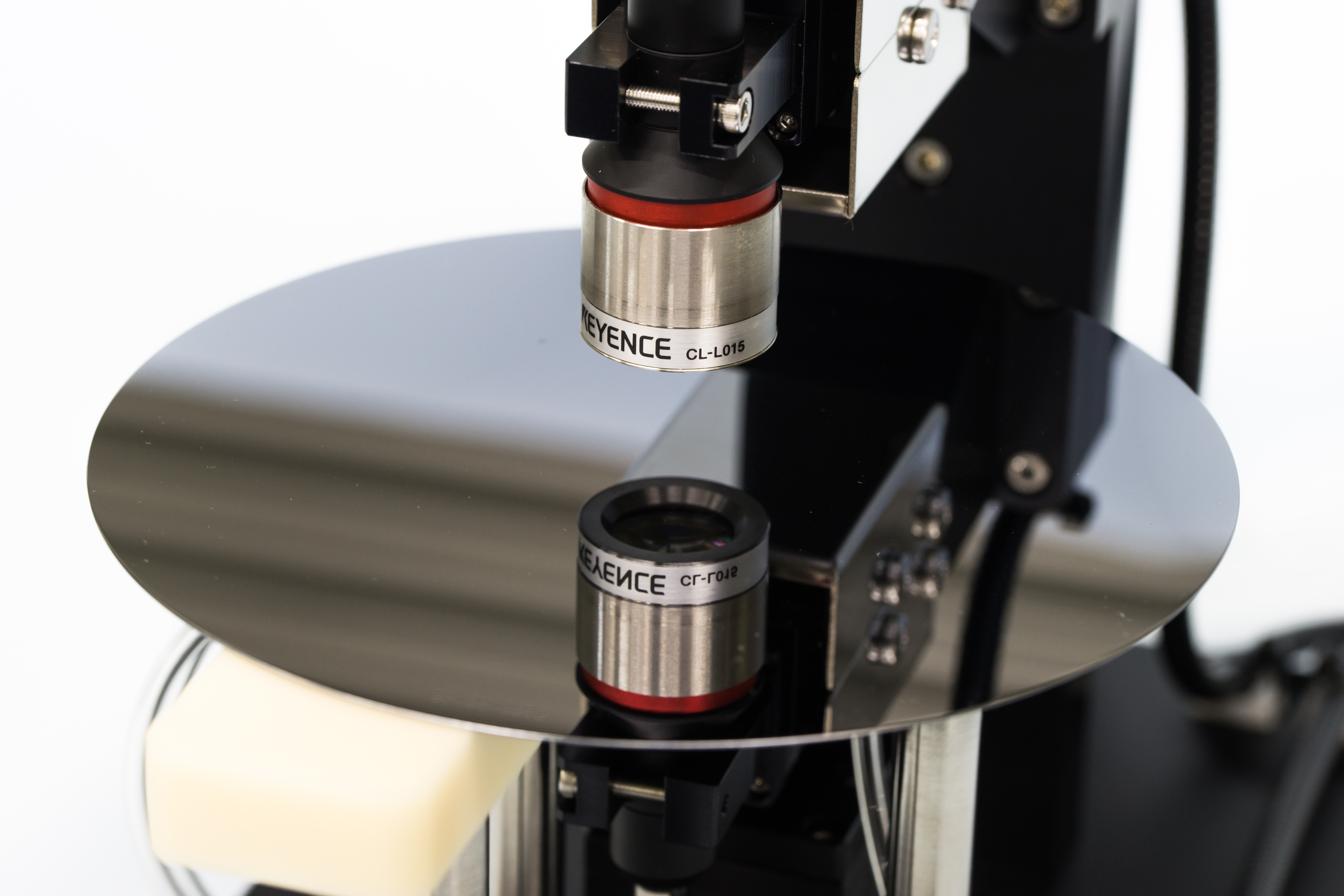
4.Since the measurement is performed with the laser sensor heads
placed opposite each other, the thickness can be measured accurately
without being affected by the lift of the object being measured.
<PERFORMANCE>
Resolution 0.01μm
Range of thickness measurement Max.10mm
Power supply AC100V 50/60Hz 3A
Weight: Approximately10kg
�
<SYSTEM BREAKDOWN>
Standard system consists of the following equipments:
| ① |
Thickness measuring equipment |
1set
|
| ② |
Table (to be selected from several
tables for your needs) |
1set
|
| ③ |
Control box |
1set
|
| ④ |
Switch box |
1set
|
| ⑤ |
Display unit (7" color LCD
touch panel) or laptop PC for measuring control |
1set
|
| ⑥ |
Connecting cables. |
1set
|
| ⑦ |
Fine adjustment gauge
(Select thickness) |
1 peace
|
| ⑧ |
Standard software for measuring
control |
1set
|
and more options are available for your own use.
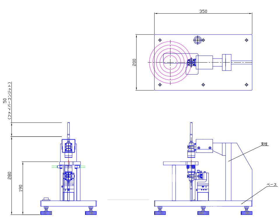
<Dimension Drawings>

(Remarks)
| *1 |
It may not be possible to measure
curvatures depending on the curvature level and stiffness.Please
contact us for further information. |
<Customization Request>
Please contact us if you need other special specifications.

NON-CONTACT THICKNESS
MEASURING DEVICE

<Send
your inquiries to>
Sasaki-koki,
Co, INC.
TOP
|


